Electron beam lithography
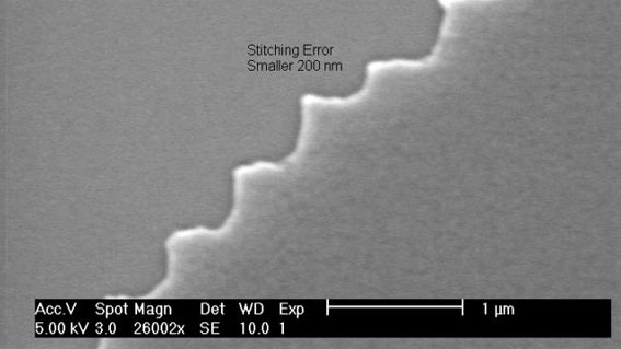
Electron beam lithography has found wide usage in mask-making for photolithography, low-volume production of semiconductor components and research & development. In many markets it is common to convert a commercially available electron microscope into an electron beam lithography system using low-cost pattern generators. The writing of large patterns, however, requires the additional installation of a stable and highly-accurate substage for stitching and pattern overlay. We offer an economical alternative to high-end lithography laser stages whilst remaining competitive in terms of stability, accuracy and repeatability.
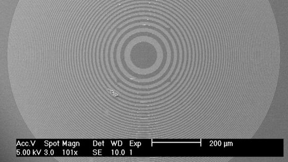
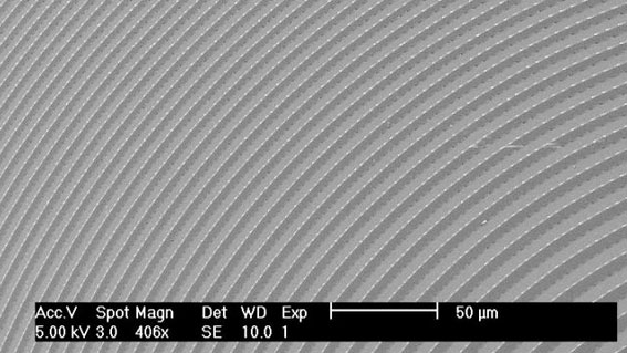
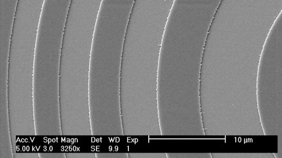
Have a look at the pictures below for an example of e-beam lithography done recently using our products.

 Back to top
 Site map