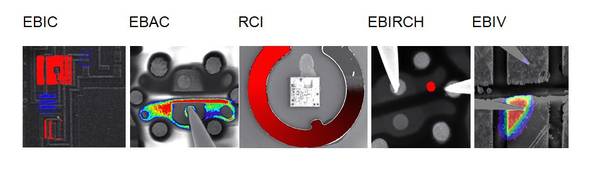
EBIC, EBAC, RCI, EBIRCH, EBIV
A powerful yet simple nanoprobing analysis technique for detecting failures in semiconductors is Electron Beam Induced Current (EBIC). EBIC as well as the related methods such as RCI, EBAC, EBIRCH, and EBIV use the electron beam to generate a signal inside a sample and the signal is then amplified for imaging purposes.
The EBIRCH technique requires two probe tips to be landed on contacts on two ends of the structure where a defect is assumed to be. One needle is biased while the electron beam scans the area of interest. At defect sites, the incident electron beam will result in localized heating, which in turn will lead to a change of resistance in the defect. This change of resistance is then visualized by the nanoprobing system, as the acquired current signal is fed back into the microscope so that a map of current flow at every position scanned by the electron beam is generated. Defects typically appear as bright spots on the map. Comparing the current map with the secondary electron image generated in parallel as well as the circuit layout, allows a determination of the defect's precise location. Tuning the electron beam's acceleration voltage provides access to various depths within the sample.
In summary, EBIRCH is performed by using:
- Resistance Contrast Imaging
- with a bias applied to the sample
- recording changes in current to the EBIC amplifier using AC mode
An advantage of these techniques over other probing techniques is that the passivation layer does not need to be removed before analysis can begin. Measurements can also be performed without damaging the surface of the integrated circuit.
Have a look at the examples below of EBIC, EBAC, RCI, and other tasks that have been done recently using our systems.


 superimposed on the corresponding SE image and line plot")

")


 Site map